Date Of Birth
1. Project Overview:
|
The purpose of the circuit designed in this project is to generate the logic required to display my date of birth on a seven segment display. The date of birth will be displayed in the MMDDYY format. In the design we have to use a common cathode seven-segment display, current limiting resistors, Karnaugh mapping to obtain the simplified logic expression, and at least one NAND and NOR logic. We will have to create the truth table and Karnaugh maps with simplified logic for each of the seven segments,create the circuit on MultiSim, and bread-board the circuit
|
2. Truth Table:
A truth table is used to show how a logic circuit responds to various combinations of inputs. If there is a number one, that shows that the input is true or if the switch is on or is a yes. If there is a number zero, that shows that the input is false or if the switch is off or is a no.
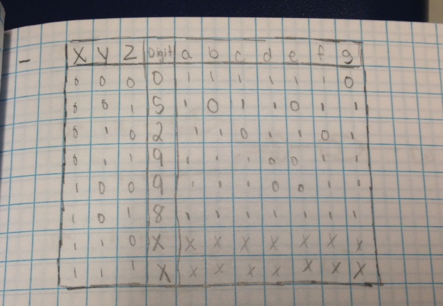
This truth table has 3 different inputs that will output a number of my date of birth. The x's represent a "do not care" condition meaning that the x can either be a zero or a one depending on whether or not you need it. The value of the x does not matter. There is an a through g column because in order for the seven segment timer to display a number the LED's need to light up to display the number. If there is a 1 under the a column, the LED representing a will light up. If there is a 0 under the column, the LED representing that letter will not light up. In order to create a 0, there needs to be an abcdef LED displayed. In order for a 5 to be displayed, there needs to be an acdfg LED displayed, and so on for the rest of the numbers. The seven LED's combined will display a number corresponding to my date of birth in the MMDDYY format. There are 8 rows because there are 3 inputs and 2^3=8.
3. Karnaugh Maps and Simplified Logic:
|
|
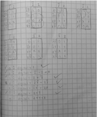
From the truth table I took the column for each letter (a-g) and made a Karnaugh map and found the simplified logic expression for each letter. I knew since there were 8 values the Karnaugh map would be 4 by 2. I inserted the numbers from the truth table in the Karnaugh map by following the rules of Karnaugh mapping. The x's resemble the don't care condition. The first two variables go vertically making the first variable 'not' the first two times and the second variables 'not' the first and last time. The third variable goes horizontally making the first one 'not'. The numbers insert in the table left to right going in the row order 1,2,4,3. My logic expression is in sum of products (SOP) form because it is easier to derive from a Karnaugh map and it's easier to create a circuit from a SOP expression. I arrived at the min-terms by looking for groups of 1's. When there are groups of 2 or 4 of ones I look for their common terms. Once I've covered all the groups of ones, I add the expressions. Using K-Mapping over Boolean Algebra is a quicker and easier way to derive the logic expressions. There is less room to make mistakes and one can usually find the expression faster. The reason there is so many expressions is because there is an expression for each LED in the seven segment display. There are seven LED's in a seven segment display and each one has its own logic expression so it can be activated when it needs to be.
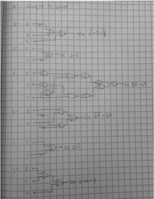
The second image is the hand drawn circuits for each logic expression of each LED in the seven segment display.
The second image is the hand drawn circuits for each logic expression of each LED in the seven segment display.
4. MultiSim Implementation:
This is the AOI logic circuit that I created to generate my date of birth. I created this circuit in MultiSim to test if my expressions were correct and if the output created my date of birth correctly. This circuit was created only using two-input gates and it follows the logic expressions shown above.
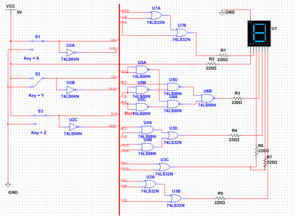
This un-simplified circuit is created in bus form to allow the creating of the circuit to be easier. To create the circuit I used 3 invertor gates (74LS04), 2 AND gates (74LS08), 6 OR gates (74LS32), and 6 NAND gates (74LS00). To build this circuit on a breadboard one would need 1 invertor chip (74LS04), 1 AND chip (74LS08), 2 OR chips (74LS32), and 2 NAND chips (74LS00). An invertor changes the input to not the input, an AND gate multiplies two inputs, and an OR gate adds two inputs. I used a NAND gate for segment D. I did this because the logic expression contained multiplication (AND gate) and addition (OR gate) so instead of needing an AND and OR gate, I just needed a NAND gate. The NAND and NOR gates are used because they are universal gates and therefore can be used to accomplish any of the basic operations. Using the NAND gate versus AOI logic for segment D saved 1 chip but the amount of gates were the same. For AOI I needed 3 invertor gates, one chip, 2 AND gates, one chip, and 1 or gate, one chip. For NAND I needed 6 NAND gates, 2 chips. It is important to conserve gates and chips because it is less expensive ,it will be quicker to create, and the current will take less time to transfer from the beginning to the end,
7 segment display is an electronic component with seven LEDs that display numbers from 0 to 9.It is available in two configurations: common cathode and common anode. All the 7 LED terminals have their own logic expression so that together they can create a number. Common Cathode has all LED grounds connected and Common Anode has all LED power connected. We are using common cathode so we can connect the 7 segment display to ground and connecte to the appropriate segment to power to light up that segment. The purpose of using resistors before the seven segment display is to limit the current going to the LED's,
7 segment display is an electronic component with seven LEDs that display numbers from 0 to 9.It is available in two configurations: common cathode and common anode. All the 7 LED terminals have their own logic expression so that together they can create a number. Common Cathode has all LED grounds connected and Common Anode has all LED power connected. We are using common cathode so we can connect the 7 segment display to ground and connecte to the appropriate segment to power to light up that segment. The purpose of using resistors before the seven segment display is to limit the current going to the LED's,
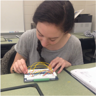
5. Bread-Boarding:
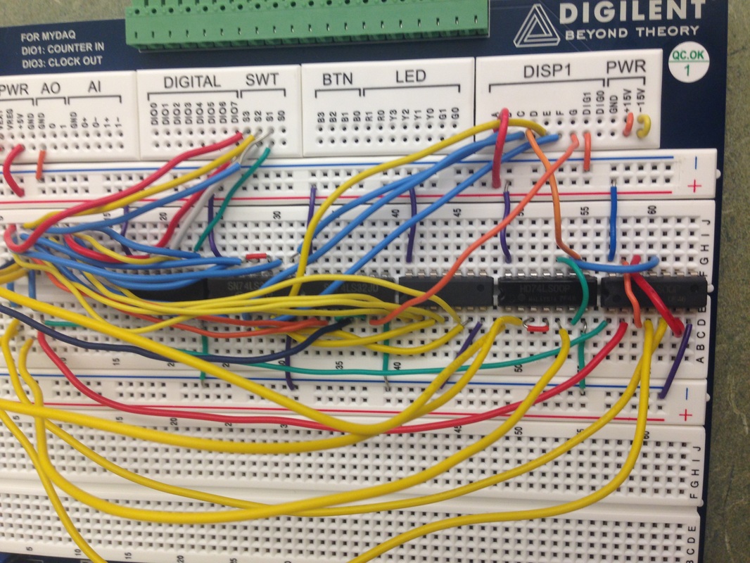
This is showing my X, Y, and Z inputs being connected to the Inverter, OR chips, AND chip, and NAND chips. Each segment has its own logic expression so there is 7 different circuits creating the whole circuit. Also shown is each chip being grounded and powered.
|
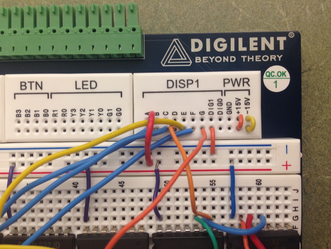
This is showing the different logic expressions going to their correct segment to activate the seven segment display.
|
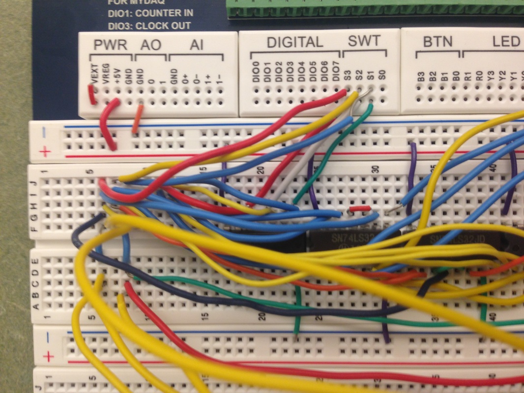
This is showing the power and ground being connected and S3 (x), S2 (y), and S3 (z) being linked to another row so I could have more access to each input.
|
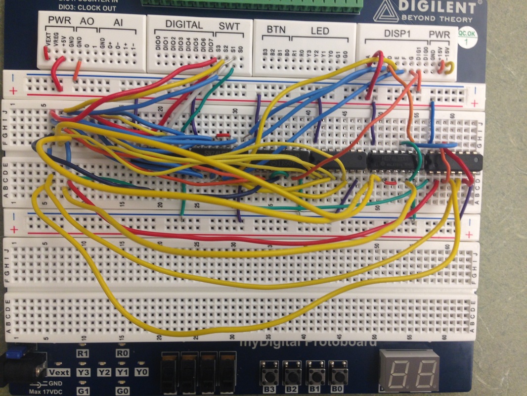
My second bread boarding experience went well. I took my circuit home to complete it over the weekend and I did it 3 times because I thought it was faulty when in reality I didn't have a proper power source, The last time I did my circuit I made it very organized and color coordinated. When I tested it in class I realized I needed to connect my A segment to power since it was always one. Once I connected it to power my bread-board was successful. This bread-board experience made me learn the importance of organization and how to take time to properly place your wires. Also I learned not to forgot anything. NAND, AND, and OR chips all include the same layout with 4 gates while the invertor has 6 gates.
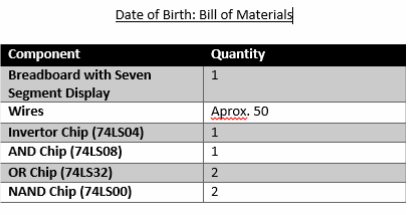
6. Bill of Materials:
|
This a bill of materials that lists all the materials that I needed to make my circuit for the majority vote project. On the left is each component utilized and on the left is the quantity of the component. I used one breadboard with seven segment display, around 50 wires, one invertor chip, one AND chip, two AND chips, and two NAND chips.
|
|
7. Conclusion:
From this project I learned how to take the numbers of my birthday and have a seven segment display display my birthday. I derived, designed, and created a circuit to fit the problem statement. After we read and understood the problem statement we had to create a truth table and then K-Mapp each segment of the seven segment display. After the K-Mapp we derived a simplified logic expression for each segment, created the circuit on MulitSim, and then bread-boarded the circuit. What I would do differently next time is take the time to make my design as efficient as possible and I would make my breadboard more organized. Overall I have no further questions about the concepts addressed in the problem; I understood the concepts of this project well. K-Mapping was useful to obtain the simplified logic expression. I didn't have to use Boolean Algebra to derive the simplified logic expression. When I K-Mapped, it was quicker, easier, and I found there was less room for mistakes. Overall this project was a great way to display circuits, K-Mapping, and seven segment displays in a fun and cool scenario incorporating a very effective way to learn the technical side of it.
